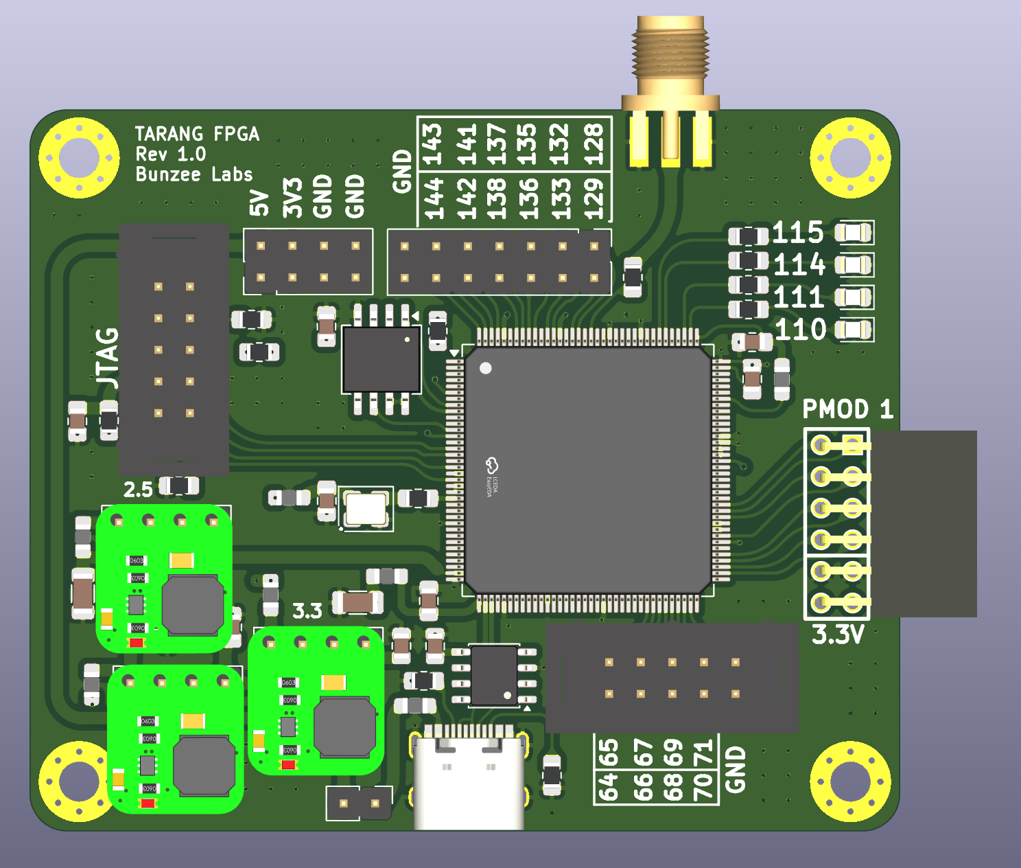
The idea is simple: build a low-cost, purpose-built HF receiver around a cheap high-speed ADC instead of repurposing an RTL-SDR.
An RTL-SDR is an excellent general-purpose radio tool, but it was not designed as a high-dynamic-range HF receiver. A direct-sampling design with proper HF preselection, controlled gain, a stable sampling clock and FPGA-based digital down-conversion should make a more interesting homebrew receiver.
The goal is not to claim IC-7300-class performance from a $25 design. The goal is to explore the same broad receiver architecture at a much lower cost and to measure honestly how well it works.
Target cost
- TARANG FPGA board, approximately 10K LUTs: under $15
- ADC daughter board, including the analog front end: under $10
- Total target cost: under $25, and possibly much less
These are initial estimates rather than a finished bill of materials.
Proposed architecture
- Hangzhou Ruimeng Technology MS9280, 10-bit, 35 MSPS pipeline ADC
- Fixed, low-jitter 35 MHz sampling clock
- Switchable HF input filters, gain and attenuation
- Small FPGA for ADC capture, digital down-conversion and decimation
- Raspberry Pi Pico 2 / RP2350 for control and USB I/Q streaming
The complete receive path would look roughly like this:
Antenna protection
  -> switched sub-octave or amateur-band BPFs
  -> 0 / 10 / 20 dB attenuation
  -> optional preamplifier
  -> transformer or differential ADC driver
  -> MS9280 ADC
  -> FPGA digital down-converter and decimator
  -> RP2350 control and USB I/Q transport
  -> SDR software on the host
This is the same broad idea used by modern direct-sampling HF radios: digitize a suitably filtered portion of the RF spectrum, then perform tuning and most of the receiver filtering digitally. Commercial radios such as the Icom IC-7300 and Yaesu FT-710 add higher-performance conversion chains, clocking, preselection, shielding, overload management and extensive DSP, but the high-level partition is similar.
A fixed sampling clock is enough
The ADC sampling clock does not need to tune with the receiver. A fixed 35.000 MHz clock is preferable, while the selected RF frequency is tuned using an FPGA numerically controlled oscillator (NCO).
Fixed 35 MHz clock
       |
       v
     MS9280
       |
       v
FPGA NCO + complex mixer
       |
       v
Selected baseband I/Q channel
A fixed clock gives predictable ADC timing, fixed decimation ratios, stable DSP filter coefficients and a consistent USB output rate. Continuously changing the sampling clock would move every alias and would complicate the entire DSP chain without helping ordinary receiver tuning.
A low-cost TCXO is a reasonable choice, provided that its phase noise and edge jitter are suitable. Frequency accuracy and sampling-clock quality are related, but they are not the same thing. A TCXO may have excellent ppm stability while still having mediocre close-in phase noise.
At 28 MHz:
1 ppm clock error   -> approximately 28 Hz tuning error
2.5 ppm clock error -> approximately 70 Hz tuning error
This can be calibrated by adjusting the NCO frequency scale in software. A fixed 1 to 2.5 ppm TCXO is therefore already adequate for ordinary SSB and CW reception, assuming the clock waveform itself is clean.
For an ideal 10-bit ADC, the aperture-jitter limit at a 28 MHz input is roughly:
SNRjitter = -20 log10(2 * pi * fin * tjitter)
Matching the approximately 62 dB ideal quantization SNR of a 10-bit converter at 28 MHz gives a rough clock-jitter target of about 4.5 ps RMS. The real ADC will have lower ENOB than an ideal converter, so this is not a hard requirement, but it shows why a clean oscillator and clock buffer matter.
A practical clock chain could be:
35 MHz TCXO or low-jitter XO
  -> clean local supply and decoupling
  -> optional low-jitter CMOS clock buffer
  -> 22 to 47 ohm source-series resistor
  -> ADC clock input
A clipped-sine TCXO may need a comparator or clock buffer. A direct CMOS-output oscillator is simpler if its phase-noise performance is acceptable. The clock source should be close to the ADC and kept away from the FPGA clock network, USB lines, switching regulators and the parallel ADC data bus.
A programmable fractional clock generator may be useful during experiments, but a fixed low-phase-noise oscillator is the cleaner default for the final receiver.
Direct sampling and undersampling
At a 35 MSPS sampling rate, the first Nyquist zone extends from DC to 17.5 MHz. Signals in this range can be represented directly, so the 20m amateur band around 14 MHz is straightforward.
The 10m band is above the first Nyquist zone, but it can be received using band-pass sampling, also called undersampling. For example:
Sampling rate: 35.000 MHz
RF input:      28.000 MHz
Digital alias: 35.000 - 28.000 = 7.000 MHz
The second Nyquist zone, from 17.5 to 35 MHz, folds into the first zone with spectral inversion. Therefore, increasing RF frequency from 28.0 to 28.1 MHz moves the alias from 7.0 to 6.9 MHz. The FPGA or host software must account for this inversion by changing the NCO direction, swapping I and Q, or reversing the displayed spectrum.
The general aliasing relationship is:
falias = abs(fin - k * Fs)
with the result folded into the range from DC to Fs / 2.
A signal appearing at 7 MHz in the sampled spectrum could have originated from several analog frequencies, including approximately:
7 MHz, 28 MHz, 42 MHz, 63 MHz, 77 MHz, ...
That is why the analog filter is essential. For 10m reception, the input path must select the desired 28 MHz region and strongly reject the other frequency bands that can alias into the same digital spectrum. The ADC's wide analog input bandwidth enables undersampling, but it also makes inadequate front-end filtering much more dangerous.
The analog front end matters more than the block diagram
A 10-bit ADC can make an excellent practical HF receiver, but only when the analog front end prevents large unwanted signals from consuming its limited input range.
A sensible front-end chain is:
Antenna protection
  -> switched sub-octave or amateur-band BPFs
  -> 0 / 10 / 20 dB attenuation
  -> optional preamplifier
  -> transformer or differential ADC driver
  -> ADC
The protection stage may include ESD protection, a limiter and provisions for receiver muting when used near a transmitter. The protection components must be chosen carefully because excessive capacitance or nonlinear junctions can degrade strong-signal performance.
The switched filters should be considered mandatory rather than an optional refinement. Possible approaches include:
- Individual amateur-band filters;
- Sub-octave filters covering several neighbouring bands; or
- A combination of broad preselection followed by a narrower 10m band-pass filter for undersampling.
The attenuator is equally important. A digital AGC operating after the ADC can make the audio level comfortable, but it cannot repair ADC clipping. The FPGA should monitor the ADC over-range indication and sample statistics, then ask the RP2350 to switch attenuation or disable the preamplifier before persistent overload occurs.
On the lower HF bands, atmospheric and man-made antenna noise is often already high enough that large amounts of preamplifier gain are unnecessary. Excessive gain only reduces blocker headroom. A modest preamplifier may still be useful on the upper HF bands, with small antennas, or when front-end filter loss and ADC noise would otherwise dominate.
The correct gain plan should be measured rather than guessed. Ideally, the antenna noise should be visible above the receiver's own noise floor without placing ordinary strong signals close to ADC full scale.
The ADC input network also needs attention. Depending on the converter input requirements, a transformer or differential amplifier may be needed to:
- Convert a 50-ohm single-ended signal to differential drive;
- Establish the required common-mode voltage;
- Present the correct ADC input amplitude;
- Isolate ADC sampling transients from the filter; and
- Maintain good linearity across the desired HF range.
The final circuit must follow the actual MS9280 input and reference requirements. Similarity to another ADC's pinout is not enough to assume an identical optimum drive network.
Why the MS9280?
The MS9280 is attractive because it combines 10-bit resolution with a 35 MSPS parallel output rate at low cost. Its published feature set and pin-level organization appear closely related to the older Analog Devices AD9280 family, which is an 8-bit, 32 MSPS pipeline ADC designed to support IF undersampling.
The two datasheets have notable similarities in supply range, package, reference and clamp functions, over-range output and pipeline architecture. However, datasheet similarity alone does not prove that the MS9280 is literally an AD9280 clone or derivative. The safe claim is that it appears to target a similar application and interface while offering 10-bit, 35 MSPS operation.
The extra resolution is useful, but it does not guarantee better reception by itself. Real performance will depend on:
- Effective number of bits at HF input frequencies;
- Aperture jitter and sampling-clock phase noise;
- Reference and power-supply noise;
- Front-end filter rejection and insertion loss;
- ADC input-driver linearity;
- PCB layout and digital coupling; and
- Overload behaviour in the presence of strong signals.
An ideal ADC has an approximate full-scale sine-wave quantization SNR of:
SNR = 6.02 * N + 1.76 dB
For 10 bits this is about 62 dB. A real low-cost converter will deliver less, especially as the analog input frequency rises.
The FPGA is effectively mandatory
The raw ADC interface produces:
35,000,000 samples/s * 10 bits = 350 Mbit/s
This is far too much data to stream directly through the RP2350's USB Full-Speed interface. The FPGA must capture the parallel ADC bus and reduce it to a much narrower complex I/Q stream before the microcontroller sees it.
A sensible division of work is:
FPGA:
  ADC capture
  offset-binary to signed conversion
  NCO
  complex mixer
  CIC decimator
  FIR compensation and channel filtering
  optional further decimation
  DC-offset removal
  AGC statistics and overload detection
  FIFO buffering toward the RP2350

RP2350:
  filter-bank selection
  gain and attenuator control
  tuning commands
  calibration storage
  FPGA register control
  USB framing
  low-rate I/Q transport
This division keeps hard real-time, sample-by-sample processing in the FPGA and leaves control-plane work to the RP2350.
Digital down-conversion
The FPGA digital down-converter converts the selected RF or aliased IF channel to complex baseband:
ADC samples
  -> multiply by cos(NCO phase) -> I
  -> multiply by sin(NCO phase) -> Q
The NCO can be built from a phase accumulator and sine/cosine lookup table, CORDIC, or another compact oscillator structure. The phase-accumulator width sets the tuning resolution. For example, a 32-bit NCO at 35 MHz has a frequency step of approximately:
35,000,000 / 2^32 = 0.00815 Hz
That is far finer than required. A smaller accumulator may therefore be used if FPGA resources are tight.
The complex mixer needs two multipliers unless a more specialized architecture is used. Many small FPGAs have dedicated multiplier or DSP blocks, which are preferable to implementing wide multipliers in LUTs.
After mixing, the wanted signal is near DC, but the stream is still running at 35 MSPS. It must be low-pass filtered before reducing the sample rate.
CIC and FIR decimation
A cascaded-integrator-comb (CIC) filter is useful for the first large reduction in sample rate because it needs adders, subtractors and registers rather than multipliers.
One convenient example is:
35.000 MSPS
  -> CIC decimate by 70
500.000 kSPS
  -> FIR decimate by 5
100.000 kSPS complex I/Q
A 100 kSPS complex stream represents approximately 100 kHz of total RF bandwidth, or roughly +/-50 kHz around the tuned centre frequency. That is wide enough for a useful panadapter slice while keeping the USB rate manageable.
At 16 bits each for I and Q:
100,000 samples/s * 2 channels * 16 bits = 3.2 Mbit/s
This is realistic over efficient USB Full-Speed bulk transfers, with far more margin than the original 350 Mbit/s stream. A wider output such as 192 kSPS is possible, but it leaves less USB and firmware headroom.
The CIC filter has passband droop, so it should normally be followed by an FIR filter that:
- Compensates the CIC droop;
- Defines the usable output passband;
- Provides stop-band rejection before the next decimation stage; and
- Optionally reduces the sample rate again.
CIC filters also have substantial internal word growth. For an N-stage CIC
with rate change R and differential delay M, the maximum gain is:
(R * M)^N
The accumulator widths must be increased accordingly, followed by deliberate rounding or saturation. Silent truncation inside the CIC can destroy weak signals or create spurious responses.
For a narrow SSB or CW receiver, the FPGA could continue decimating to a much lower rate and even perform demodulation. For a general SDR design, however, streaming a 50 to 100 kHz complex slice to a host gives more flexibility and keeps the FPGA design manageable.
Decimation and processing gain
A narrow digital filter integrates much less wideband quantization and thermal noise into the final receive channel. The theoretical processing gain from reducing the first-Nyquist-zone bandwidth to a 2.4 kHz SSB channel is approximately:
10 log10(17.5 MHz / 2.4 kHz) = 38.6 dB
This is one reason a modest-resolution high-speed ADC can still produce good narrowband reception after digital filtering.
Processing gain does not increase ADC overload headroom. A strong signal inside the selected analog preselector passband can still clip the ADC even if that signal is far outside the tiny digital channel being listened to. Analog filtering, attenuation and gain control therefore remain essential.
Expected FPGA size
A single receiver channel should be practical in a small FPGA if the device has sufficient block RAM and hardware multipliers. The main resources are likely to be:
- Parallel ADC input registers;
- NCO phase accumulator and lookup storage;
- Two digital multipliers;
- CIC integrator and comb registers;
- FIR coefficients and multiply-accumulate resources;
- Output FIFO; and
- Control and overload-monitoring logic.
The CIC stage is inexpensive in multipliers but can consume many register bits. The FIR may be time-multiplexed after the first decimation because its clock rate is then much lower. Whether everything fits comfortably in the TARANG FPGA board depends on the exact FPGA's DSP blocks, memory and routing, not just its headline LUT count.
Is this really better than an RTL-SDR?
Potentially, for HF use - but this must be demonstrated by measurement.
The advantages should be:
- A purpose-built HF input path;
- Real switched preselection;
- Direct sampling rather than relying on an HF upconverter;
- 10-bit conversion rather than the usual 8-bit RTL-SDR path;
- Deterministic FPGA decimation; and
- Full control over the gain plan, clock and DSP chain.
The risks are equally real:
- The low-cost ADC may have disappointing ENOB or spurious performance;
- Clock phase noise may limit close-in reception;
- 10-bit instantaneous dynamic range is still modest;
- Poorly designed input filtering may make undersampling unusable;
- FPGA or PCB digital noise may couple into the ADC; and
- USB framing or buffering errors may cause dropped I/Q samples.
It would be premature to call the design better than an RTL-SDR until the two receivers have been compared under the same antenna, bandwidth and signal conditions.
Initial measurement plan
The first prototype should be evaluated methodically rather than only by listening to signals.
ADC and clock
- Confirm the sampling frequency and temperature drift.
- Measure the clock waveform at the ADC without excessively loading it.
- Feed a clean test tone and estimate SNR, SINAD, SFDR and usable ENOB.
- Repeat at several input frequencies, including 7, 14 and 28 MHz.
- Check whether clock-source or supply changes move visible spurs.
Analog front end
- Measure each filter's insertion loss and stop-band rejection.
- Verify 10m alias rejection against 7 MHz and other corresponding zones.
- Determine the ADC full-scale input level through each gain setting.
- Measure the preamplifier and attenuator linearity.
- Test protection and receiver muting near a transmitter before antenna use.
Receiver performance
- Measure minimum discernible signal in several bandwidths.
- Perform two-tone intermodulation tests.
- Test blocking from a large signal inside and outside the selected BPF.
- Record the level at which the over-range output begins to trigger.
- Verify that attenuation control reacts before sustained clipping.
- Compare sensitivity and overload behaviour with an RTL-SDR using identical filters and bandwidths.
Digital path
- Verify NCO frequency accuracy and spectral orientation in each Nyquist zone.
- Check CIC word growth, rounding and saturation with full-scale inputs.
- Measure FIR passband flatness and stop-band rejection.
- Run long USB streaming tests and count FIFO overflows or dropped packets.
Status
To be built and tested.
The architecture is credible, but the interesting part is not the block diagram. The real project is the strong-signal analog front end, clean clock, careful ADC layout, mathematically correct decimation and honest receiver measurements.
AD9280 reference datasheet
TARANG FPGA R1.0